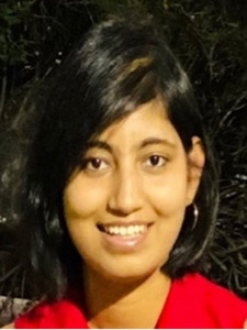
OSE Dissertation Defense by Ms. Subhashree Seth on Photonic Crystal Surface Emitting Lasers (PCSELs) based on Dot in Well (DWELL) Active Region by Epitaxial Regrowth Method
Departmental News

Posted: April 1, 2025
Date and Time: Friday, April 4, 2025, from 2:00 PM - 3:30 PM
Location: CHTM, Room 103
Dissertation Committee:
Prof. Ganesh Balakrishnan, EPSCoR Director and Department of Electrical and Computer Engineering (Committee Chair)
Prof. Daniel Feezell,Department of Electrical and Computer Engineering
Prof. Nathan Jackson,Department of Mechanical Engineering
Prof. Thomas J. Rotter,Department of Electrical and Computer Engineering
Dr. Sadhvikas Addamane,Sandia National Labs & CINT
Abstract:
The most common forms of semiconductor lasers are the edge-emitting laser (EEL) or the vertical cavity surface emitting laser (VCSEL). Conventional EELs exhibit multi-longitudinal-mode emission along with highly divergent, astigmatic, and non-diffraction limited beams. On the other hand, VCSELs offer narrow symmetric beams, and catastrophic optical damage (COD)-free operation. The downside of VCSELs is that the small dimension of the emission area limits the single-mode output power to a few milliwatts. Therefore, achieving high power with high beam quality is challenging for both EELs and VCSELs. In this study, we make use of a different laser architecture to realize vertically emitting lasers – the photonic crystal surface emitting laser (PCSEL). The PCSEL can simultaneously achieve high beam quality, high room temperature continuous wave output power, compact form factor, and electrical injection, with less fabrication complexity. In 1999, Noda et al. and Meirer et al. independently proposed a two-dimensional (2D) photonic crystal as the laser cavity of a semiconductor laser. PCSELs have been fabricated using various techniques, such as wafer fusion, deposition of conducting layers over the “PC-slab-on-substrate,” and epitaxial regrowth. Among these methods, epitaxial regrowth has emerged as a promising approach due to its ability to eliminate light-absorbing defects, improve device yield, and enhance overall device performance.
In this thesis, self-assembled quantum dots (QDs) embedded in InGaAs quantum wells (QWs) are employed as the active regions for photonic-crystal surface-emitting lasers (PCSELs). Previously reported QD PCSELs were fabricated by depositing a conductive layer over the “PC-slab-on-substrate” and utilizing deep etching photonic crystal techniques. However, there are a few recent studies that combine QD active regions with the epitaxial regrowth process, which presents new opportunities for further improvements in device performance. During the regrowth process, the material is subjected to high growth temperatures exceeding 600°C, which can unintentionally lead to the annealing of the QD-based active region. This annealing effect can alter the quantum dots (QDs), changing their size and resulting in a blue shift in photoluminescence (PL) and narrowing of the PL emission. Such changes misalign the gain peak with the cavity resonance, thereby diminishing lasing performance. As dot-in-well (DWELL) active regions are known to exhibit better thermal stability than both QDs and QWs, they could serve as an ideal candidate for regrown photonic crystal surface-emitting lasers (PCSELs).
DWELL PCSELs at 1230 nm were fabricated using epitaxial regrowth. The epitaxial growth process was conducted through electron beam lithography (EBL) and inductively coupled plasma (ICP). Molecular beam epitaxy (MBE) was explored as a growth medium for both the initial growth and regrowth phases. The challenges associated with surface issues during MBE regrowth are also discussed, along with the potential benefits of MOCVD regrowth. The difficulties introduced by high-temperature regrowth are addressed, and solutions to these challenges are explored.
Finally, the fabricated samples were studied using optical pumping and studied by electrical injection, with standard device processing techniques. Additionally, an innovative indium bump flip-chip bonding process was explored to facilitate the fabrication of these PCSEL devices. Surface emission was collected from the backside through the substrate, enabling effective performance measurement.
Biography:
Subhashree Seth received the B.Sc in Physics (Honours) from, Lady Brabourne College, University of Calcutta, India and M.Sc in Applied Physics from IIT(ISM) Dhanbad, India. She is currently pursuing the Ph.D. degree in Optical Science and Engineering at The University of New Mexico (UNM), USA. Since 2019, she has been working as a Research Assistant under the guidance of Prof. Ganesh Balakrishnan. Her current research interests include nanophotonics, optoelectronics and semiconductor lasers. She has been working on the development of high-power photonic crystal surface emitting lasers.
